


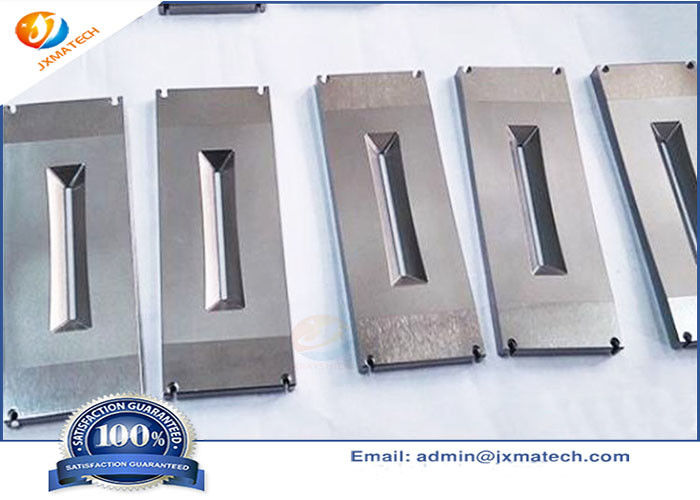


Molybdenum High Temperature Alloy TZM Rod


|
Product Details:
|
|
| Place of Origin: | CHINA |
|---|---|
| Brand Name: | JINXING |
| Certification: | ISO 9001 |
| Model Number: | Moly Ion Implanting Parts |
|
Payment & Shipping Terms:
|
|
| Minimum Order Quantity: | 15 kg |
| Price: | Negotiable |
| Packaging Details: | plywood cases |
| Delivery Time: | 15-20 days |
| Payment Terms: | L/C, T/T, D/P, Western Union |
| Supply Ability: | 2000 kg per month |
|
Detail Information |
|||
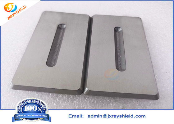
| Product Name: | Moly Ion Implanting Parts | Grade: | Mo1 |
|---|---|---|---|
| Density: | 10.2 G/cm3 | Purity: | >=99.95% |
| Tensile Strength: | >325 MPa | Elongation: | <21% |
| Standard: | ASTM B387-01 | Application: | Semiconductor Industry |
| Highlight: | Ion Implanting Molybdenum Products,Molybdenum Ion Implanting Parts,Semiconductor Ion Implanting Parts |
||
Product Description
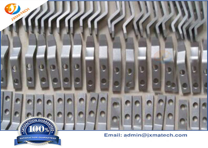
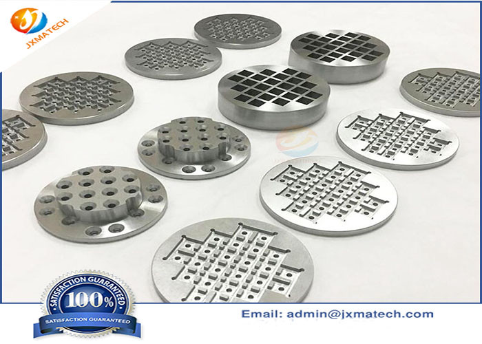
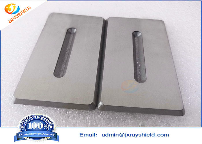
Moly Ion Implanting Parts are an ion beam technology that ionizes the atoms of an element into ions, accelerates them at a voltage of tens to hundreds of kV, and injects them into the surface of workpiece material placed in vacuum target chamber after obtaining high speed.
After ion implantation, the physical, chemical and mechanical properties of the surface of the material will change significantly. The continuous wear resistance of the metal surface can reach 2 ~ 3 orders of magnitude of the initial implantation depth.
SPECIFICATION & CHEMICAL COMPOSITIONS (NOMINALS)
| Material | Type | Chemical Composition (by wt.) |
| Pure Moly | Mo1 | >99.95%min. Mo |
| Ti-Zr-Mo Alloy | TZM | 0,5 % Ti / 0,08 % Zr / 0,01 - 0,04 % C |
| Mo-Hf-C | MHC | 1,2 % Hf / 0,05 - 0,12 % C |
| Moly Rhenium | MoRe | 5,0 % Re |
| Moly Tungsten | MoW20 | 20,0 % W |
| Moly Tungsten | MoW50 | 50,0 % W |
(1) It is a pure pollution-free surface treatment technology;
(2) It does not need thermal activation and high temperature environment, so it will not change the overall dimension and surface finish of the workpiece;
(3) Ion implantation layer is a new surface layer formed by a series of physical and chemical interactions between ion beam and substrate surface, and there is no peeling problem between it and substrate;
(4) There is no need for machining and heat treatment after ion implantation.
In semiconductor technology, ion implantation has high-precision dose uniformity and repeatability. It can obtain ideal doping concentration and integration, greatly improve the integration, speed, yield and service life of the circuit, and reduce the cost and power consumption. This is different from chemical vapor deposition.
In order to obtain ideal parameters, such as film thickness and density, chemical vapor deposition needs to adjust equipment setting parameters, such as temperature and air flow rate, which is a complex process.
In addition to the semiconductor production industry, with the rapid development of industrial control automation, ion implantation technology is also widely used in the improvement of metals, ceramics, glass, composites, polymers, minerals and plant seeds.
Enter Your Message
JINXING MATECH is an expert provider on the metal solution. Especially on the products such as Tungsten Alloy , Tungsten copper , Titanium , Zirconium, Vanadium, Hafnium, Sputtering target , Nobel metal etc,
| JINXING MATECH CO LTD |
| NO.57 KEXUEDADAO ROAD |
| 86-371-18137338517 |
| admin@jxmatech.com |